Technological Frontier: TSMC CoWoS Packaging A1
The Future of Packaging Gets Blurred – Fan-Out, ABF, Organic Interposers, Embedded Bridges – Advanced Packaging Part 4
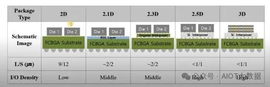
The blurring lines of 2.1D, 2.3D, and 2.5D advanced packaging. At IMAPS 2022, many advancements in this field were showcased, and the future of the advanced packaging industry is very dynamic. To briefly review, there are currently four major categories of advanced packaging.
3D = active silicon stacked on active silicon - the most famous form isAMD 3D V-Cache using TSMC's SoIC CoWandGraphcore IPU BOW using TSMC's SoIC WoW。
2.5D = active silicon stacked on passive silicon - the most famous form isNvidia AI GPU with HBM memory using TSMC CoWoS-SandIntel Meteor Lake CPUs using Intel Foveros。
Fan-out RDL (Epoxy Molding Compound Laminate) – the most famous form isTSMC's InFO, used in Apple's A-series, S-series, and M-series chips, ASE FoCoS, and Amkor WLFO. The panel layer is being developed by multiple companies.
Build-up ABF substrates (copper core covered with Ajinomoto build-up film and RDL layers) – the most famous form isIntel and AMD PC and data center chips。

In most advanced packaging, build-up ABF substrates are still used. These substrates are called hybrid substrates.
Another area of ambiguity in advanced packaging is that engineers often use the term “organic substrate.” Both ABF and core fan-out contain organic epoxy chemistries.
While the categorization from 2.5D to 3D may seem simple, the number of packaging options available is vast, blurring the lines between 2.3D and 2.1D. Furthermore, as 2.3D and 2.1D packaging capabilities evolve, the market share of 2.5D will gradually decline.
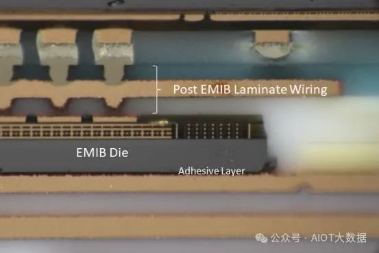
Intel's EMIB is to place a silicon bridge in the cavity of the ABF substrate. Its main purpose is to avoid the use of expensive silicon interposers and make the package beyondMask LimitEMIB isn't technically 2.5D packaging, but it does bring many of the purported benefits. How does it compare in terms of cost and performance to pure 2.5D silicon interposers or high-density fan-out? The jury is still out on future generations, but the first generation isn't dominant.
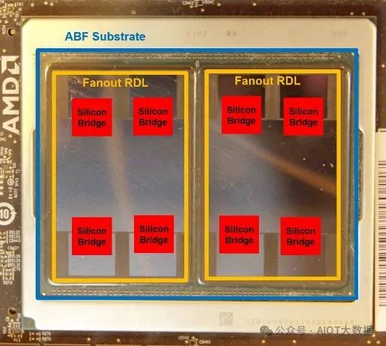
AMD's MI250X GPU (as noted above) and Apple's M1 Ultra are examples of multiple package types in the same product. Instead of a silicon interposer, a silicon bridge connects the GPU die to each HBM. Fan-out with embedded bridges is similar to Intel's EMIB, but the manufacturing process is completely different, with fan-out RDLs and a built-up substrate.
For the MI250X, two separate fan-out RDL components are packaged on top of a large ABF substrate with the silicon bridge and GPU/HBM.
While this approach is theoretically less expensive due to minimizing the use of expensive silicon interposers, the potential for yield loss is higher compared to traditional 2.5D silicon interposers.
Fan-out RDL is not a single process. It can be built using many different types of materials. Furthermore, it can be an RDL-first or chip-first flow.
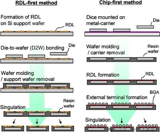
Whether fan-out RDL uses an RDL-first or chip-first process flow, the finished hybrid substrate cannot be tested before chip placement. Using a fan-out-to-substrate bonding process can result in the loss of good chips. While fan-out RDL offers theoretically lower costs, especially for panel-level fan-out, yield loss is a major reason for the continued use of silicon interposers. These yield issues can extend to substrate warpage due to coefficient of thermal expansion (CTE) mismatches between the fan-out RDL material, the build-up substrate, and the silicon.
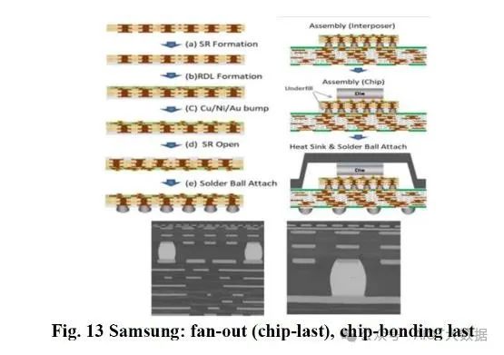
Samsung, Shin Kong, Unimicron, SPIL, and TSMC have been developing packaging processes that begin with fan-out RDL fabrication; this is then bonded to a build-up ABF substrate. The bonded hybrid substrate is then tested, and finally the chip is bonded. This is called fan-out (RDL-first or chip-last), followed by chip bonding. Each company has its own approach, with some using organic or inorganic materials. Having a known high-quality substrate for advanced packaging improves assembly yield and logistics, a significant advantage.
The data center and PC industries have traditionally employed a supply chain that matches a known-good substrate with a known-good die. RDL first/die bond last is the preferred packaging approach if it can be done cost-effectively.
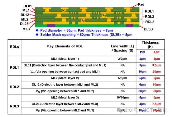
Compared to fan-out (die-last or RDL-first) processes, fan-out (chip-first) processes offer simpler and lower-cost IC integration. However, chip-first means that packaging yields are reduced by a larger number of known-good dies. As the industry transitions to more expensive process technologies, this packaging yield loss continues to be a major factor in the increasing cost of packaging processes. Fan-out (chip-last) integration also offers other advantages, such as larger die sizes, larger packages, fewer die shift issues, and finer metal length/spacing (L/S) in RDLs. L/S refers to the width of the metal interconnects and the space between them.
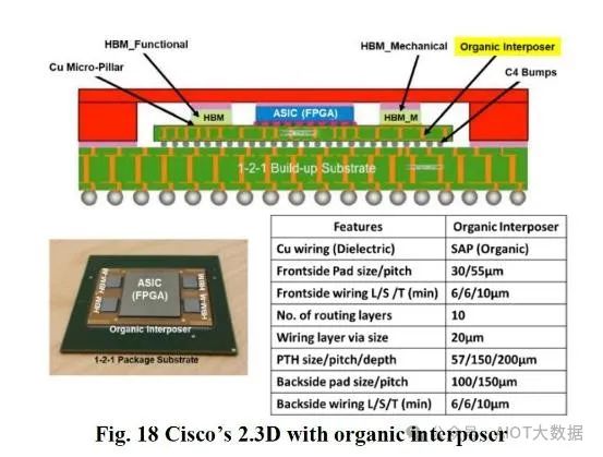
Furthermore, non-fan-out technologies are also improving. Cisco has demonstrated research related to coreless organic substrates. The main manufacturing steps for this organic interposer are the same as for build-up package substrates, except without the copper core. Compared to standard build-up ABF substrates with cores, Cisco has demonstrated 10 routing layers and a higher L/S density.
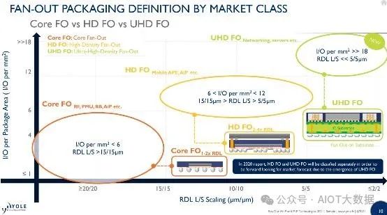
Today, L/S densities for build-up ABF substrates are as high as 10 microns; Cisco research shows that L/S for organic substrates can be reduced to 6 microns. The L/S for the core fan-out market is in the 15 micron range. Some advanced fan-outs, such asAMD 的 RDNA 3 GPUandMediaTek network processor, which can be reduced to 2 microns L/S. EMIB achieved 5 microns L/S in the first generation, and is rumored to reach 2 microns L/S in future generations.
As ABF substrates improve, the core fan-out and HD fan-out markets are gradually being eroded beyond mobile applications. Regarding dielectric materials, photoimageable dielectrics (PIDs) are now capable of achieving even finer pitches. Nevertheless, ABF still offers many advantages in terms of surface variations, as demonstrated by Unimicron.

Unimicorn intends to stick with its improved ABF technology, as it is its core competency. Fine-pitch coreless ABF adheres to its existing business model of providing known-good (hybrid) substrates. They can achieve 3µm L/S with improved surface variation, enabling scalability to higher layer counts. Their coreless ABF substrate is likely to be very competitive with current advanced fan-out processes. Because it is produced on a panel, it is competitive with wafer-level and close to future panel fan-out processes. While limited to three RDL layers, scaling to higher layers is easier than with fan-out RDL.
Coreless ABF substrates are thicker, which may be a problem for mobile applications, but for high-performance applications, reliability and performance should be better.
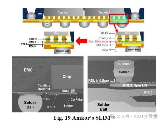
When pursuing L/S, Amkor SLIM and ASE SPIL NTI can achieve 0.4µm and 0.5µm respectively. Both are limited to these fine pitches on the first layer.
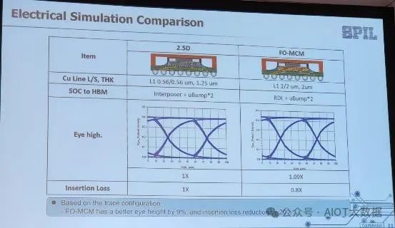
ASE SPIL says its fan-out RDL outperforms 2.5D advanced packaging and can be used to integrate HBMThe chip connects to the SOC. ASE SPIL claims its improved eye height reduces losses, allowing for higher signal rates and lower noise through the package.
While build-up ABF substrates will remain the foundation of the advanced packaging market, their performance and density are improving with the transition to coreless substrates. Furthermore, these ABF-based substrates can achieve higher layer counts, as demonstrated by Cisco, thanks to the superior surface variation characteristics demonstrated by Unimicron. In many use cases, ABF substrates are catching up to and surpassing fan-out RDL.
As RDL fan-out processes expand into applications previously reserved for 2.5D interposers, cost and yield become crucial factors. Fan-out processes using silicon bridges are becoming increasingly common, but new bridge-free processes for integrating ASICs with HBMs are nearing production. These advances in fan-out processes and ABF substrates are rapidly blurring the lines between advanced packaging.
When evaluating advanced IC packaging in the 2.1D to 2.5D space, multiple variables need to be considered. Pad pitch, L/S, and layer count are important factors, but reliability, warpage issues, packaging cost, yield, and package size also come into play. In the future, hybrid substrates—coreless ABF substrates packaged on top of standard build-up ABF substrates—may be the best option for some use cases. In other cases, die-first fan-out RDLs packaged on top of standard build-up ABF substrates may be the best option for another use case. With the proliferation of heterogeneous integration with diverse chip counts and types, the trade-offs involved in packaging are becoming increasingly difficult to evaluate.
Hybrid Bonding Process Flow – Advanced Packaging Part 5
BESI、EV Group、AMAT、TEL、ASMPT、SET、芝浦、SUSS Microtec
Hybrid bonding will be the most transformative innovation in semiconductor manufacturing since EUV. In fact, its impact on the design process will be even greater than EUV itself, from package architecture to cell design and layout. The IP ecosystem will undergo a dramatic shift, as will the manufacturing process. While 2D transistor scaling will continue, albeit at a slower pace, hybrid bonding will usher in a new era where chip designers will think in 3D.
As this hype song comes to an end, it’s important to note that bringing hybrid bonding to market at scale faces significant engineering and technical challenges, as it’s currently limited to a few AMD chips, CMOS image sensors, and 3D NAND from a few suppliers. This transition will reshape supply chains and design flows.
We will start fromBaseWe begin our coverage of high-level aspects of hybrid bonding, including process flows, tools, design use cases, challenges, and wafer-to-wafer and die-to-wafer costs. We also present our proprietary adoption model, which covers usage, tool requirements, and volumes across various markets (mobile devices, client PCs, data center CPUs, AI accelerators, HBM, etc.), as well as company-level adoption by the end of 2020.
The last major paradigm shift in packaging history was the transition from wire bonding to flip-chip. Since then, more advanced packaging formats, such as wafer-level fan-out and TCB, have been incremental improvements on the same core principle. These packaging methods all use some form of solder-bumped interconnects between the silicon die and the package or circuit board. These technologies can be scaled down to approximately 20-micron pitch.
The primary package types and process flows discussed so far in this multi-part advanced packaging series have been at the 220-micron to 100-micron scale, primarily using solder as the dielectric between the various copper interconnects on the chip. Scaling further requires another paradigm shift: bumpless interconnects using hybrid bonding. Hybrid bonding scales beyond 10-micron interconnect pitches, with plans to expand to 100 nanometers, without the use of any higher-resistance intermediates like solder.
Instead, interconnects between different chips or wafers are made directly through copper vias. Direct copper connections mean significantly less resistance when sending data to individual chips, and therefore less power consumption. This, combined with the orders of magnitude increase in the number of connections, necessitated a complete rethinking of the design.
Recap of Part 1What's the focus of advanced packaging? We can see that advances in packaging technology are aimed at achieving higher interconnect density (more interconnects per unit area) and reducing trace lengths to lower latency and energy per bit. We can see how hybrid bonding addresses both of these issues: trace lengths are significantly shortened, so latency is as low as possible without requiring on-chip global rounding, and in some cases, even shorter than on-chip global rounding, and interconnect pitch can be well below 10 microns to increase density.
What exactly is hybrid bonding?
Hybrid bonding is used for vertical (or 3D) chip stacking. Its defining feature is its lack of bumps. It eschews solder-based bumping technology in favor of direct copper-to-copper connections. This means the top and bottom chips are flush with each other. Both chips have only copper pads, not bumps, enabling ultra-fine pitch scaling. The absence of solder eliminates solder-related issues.
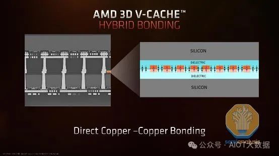
The image above shows a cross-section of AMD's 3D V-Cache, which utilizes TSMC's SoIC-X die-to-wafer hybrid bonding. The bonding interface between the top and bottom silicon is the hybrid bond layer, which sits atop the silicon die's metal layer. The hybrid bond layer is a dielectric (most commonly SiO or SiCN today) topped with copper pads and vias, typically with a pitch of less than 10 microns.
The dielectric isolates each pad, preventing signal interference between them. The copper pads are connected to the chip's metal layer via through-silicon vias (TSVs). TSVs are required to carry power and signals to the next chip in the stack. Because the bottom chip is placed face-down, these vias are needed to connect the metal layer on the top chip, through the transistor layer, and to the metal layer on the bottom chip.
It is through these copper pads that signals communicate between chips. This bonding is called "hybrid" because it combines dielectric-to-dielectric bonding and direct copper-to-copper bonding. No additional adhesives or materials are required between the bonding interfaces.
Key process conditions
Compared to previous bump-based interconnects, this introduces a whole new set of technical and process challenges. To achieve high-quality bonds, stringent requirements are placed on surface smoothness, cleanliness, and bond alignment accuracy. We'll begin by describing some of these challenges, as the process flow is designed to mitigate them. Keeping these in mind will help you better understand the process's characteristics and the advantages and disadvantages of different approaches.
Particles and cleanliness
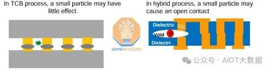
In any discussion of hybrid bonding, particles are mentioned. This is because particles are the enemy of yield in hybrid bonding. Since hybrid bonding involves bonding two very smooth and flat surfaces flush together, the bond interface is sensitive to the presence of any particles.Very sensitive.
Particles only 1 micron highThis results in a bond gap of 10 mm in diameter., which leads to bonding defects. For bump-based interconnects, there is always a gap between the device and the substrate due to the use of underfill or non-conductive film, and the gap can tolerate some particles.
Maintaining cleanliness is crucial and very challenging. Many steps, such as wafer dicing, grinding, and polishing, generate particles. Any type of friction also generates particles, which is a problem, especially since hybrid bonding involves mechanically picking up and placing the die on top of other dies. There's a lot of movement in the tooling from the die bond head and die flipper. Particles are unavoidable, but several techniques can mitigate the impact on yield.
Of course, wafer cleaning is performed regularly to remove contaminants. However, cleaning is not perfect and cannot remove 100% of contaminants in one go, so it is best to avoid contaminants in the first place. The cleanrooms required for hybrid bonding are much more advanced than those required for other forms of advanced packaging.
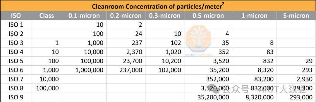
Therefore, hybrid bonding typically requires Class 1/ISO Class 3 or higher cleanrooms and equipment. For example, TSMC and Intel are striving to achieve ISO Class 2 or ISO Class 1. This is a key reason why hybrid bonding is considered a "front-end" process—it occurs in a fab-like environment, rather than that of a traditional packaging and assembly company (OSAT). Given these increased cleanliness requirements, hybrid bonding is difficult for OSATs to perform. Most OSATs would need to build newer, more advanced cleanrooms if they wanted to participate in hybrid bonding, while companies like TSMC and Intel can use older fabs or build them to similar standards as existing ones.
The hybrid bonding process also involves many tools traditionally reserved for the exclusive use of foundries. Outsourced assembly and test companies (OSATs) such as ASE and Amkor have relatively limited experience with chemical vapor deposition (CVD), etching, physical vapor deposition (PVD), electrochemical deposition (ECD), chemical mechanical planarization (CMP), and surface treatment/activation.
Cleanliness requirements and increased tooling lead to significant cost increases. Compared to other forms of packaging, hybrid bonding is not cheap. We will describe the process flow below.
Smoothness
The surface smoothness of the hybrid bonding layer is also extremely critical. The HB interface is also sensitive to any surface topography, which can lead to voids and ineffective bonding. Generally, the surface roughness threshold for dielectrics is 0.5nm, and for copper pads, 1nm. Achieving this smoothness requires chemical mechanical planarization (CMP), a key process for hybrid bonding.
After polishing, this smoothness needs to be maintained throughout the entire process. Any steps that could damage this surface, such as harsh cleaning, should be avoided. Even wafer sorting probes need to be adjusted to avoid damaging the surface.
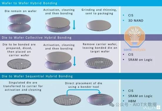
Wafer-to-wafer (W2W) or chip-to-wafer (D2W)
First, let's discuss wafer-to-wafer (W2W) or die-to-wafer (D2W) bonding. Hybrid bonding can be accomplished using either wafer-to-wafer (W2W) or die-to-wafer (D2W) processes. W2W involves directly bonding two fabricated wafers together. W2W offers higher alignment accuracy, throughput, and bonding yield. Given its relative ease, the vast majority of hybrid bonding is currently accomplished using W2W.
The higher yield of W2W bonding is due to the separation of the alignment and bonding steps. In a W2W tool, a separate chamber is used to perform alignment. Once the top and bottom wafers are aligned, they are moved into the bonding chamber (under vacuum), where they are pressed together with a slight force. After about 20 minutes, the initial pre-bond is formed.
The key to W2W is that it's a cleaner process with fewer steps. Before alignment and bonding, the wafers can be cleaned to remove most particles. Die separation (a source of particle contamination) occurs only after bonding. Because it's a wafer-level process, the alignment step also takes more time, so longer alignment times don't hurt yields as much as they would with chip-level processes.
There's also little movement within the cavity, resulting in less contamination. Currently, W2W bonders can achieve alignment accuracy below 50nm. W2W bonding is a mature process and affordable. This is evidenced by its widespread adoption in mass-market products such as 3-layer image sensors and NAND.
W2W bonding is great, but a major limitation is the inability to perform wafer sorting to select known good die (KGD). This can lead to undesirable outcomes where defective dies are bonded alongside good dies, wasting high-quality silicon.
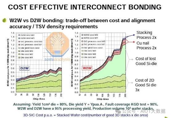
Given this, W2W is used for wafers with higher yields, which typically translates to smaller designs. In the figure below, we can see the relationship between die area and cost for W2W and D2W. The smaller the wafer size, the cheaper W2W is because the wafer yield is higher. However, as wafer size increases, the W2W cost curve becomes steeper, primarily due to the cost of lost good wafers. As die size increases, the proportion of good wafers per wafer decreases, resulting in a higher number of defective and good wafers.
We can see that W2W is used for smaller chips with high production volume: CMOS image sensors,3D NAND, and so far only used forGraphcore Bow IPUlogic.
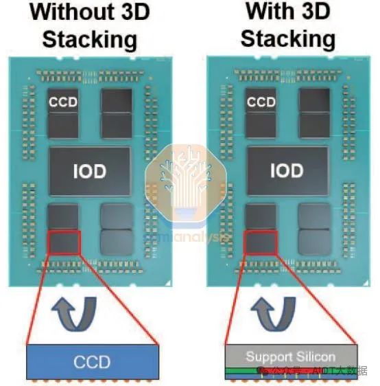
While the Graphcore Bow IPU is a larger HPC chip, the top die is not leading-edge logic but rather a passive capacitor die for power delivery, so its yield should be quite high and the silicon cheaper. Another drawback of W2W is that the top and bottom dies must be the same size, thus limiting the flexibility of heterogeneous integration options.
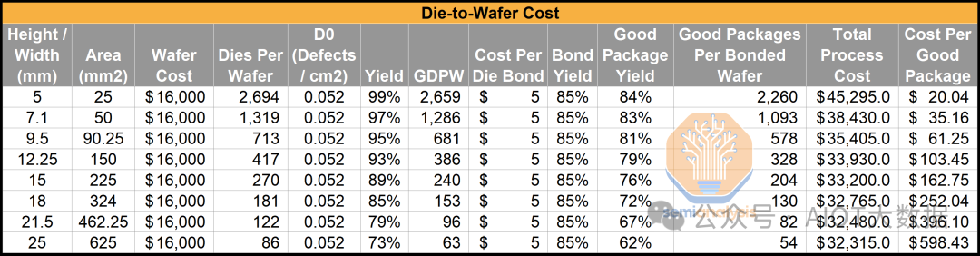
Cost is influenced by many factors. Key factors include wafer cost, D0 (defect density), and bonding yield. Each factor can increase or decrease costs. Please note that these are example numbers used to emphasize the point. Do not use the table below, as it does not reflect the actual cost of bonding. To understand the actual costs of today's products, please contact us for the AMD MI300X cost report or the Zen 3, Zen 4, and Zen 5 hybrid bonding cost report.
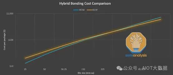
As you can see, D2W is more expensive for small chips, but the opposite is true for larger chips. W2W is more expensive. Being able to test and bond known good dies (KGD) without risking defect accumulation and wasting good silicon is crucial, which is why die-on-wafer (D2W) was the first approach to achieve productization. It can handle poor yields and still produce a commercially viable product.
To overcome these limitations, D2W bonding is required. D2W bonding is more challenging. After wafer sorting, the KGDs are separated from the top wafer and individually attached to the bottom wafer using a pick and place tool. This presents a greater bonding challenge, as each wafer requires more bonding steps. These additional steps introduce more particle contamination, particularly from die separation and movement of the bond head during pick and place.
D2W can be a "collective" process, where the KGD is aligned and first temporarily bonded to a reconstituted carrier wafer. The reconstituted carrier wafer is then bonded to the substrate for the actual pre-bonding. This is done to separate alignment and bonding, as with W2W, and allows for a cleaning step to remove any accumulated contaminants before the final pre-bonding. The downside is the additional steps involved, and the additional W2W bonding step increases the likelihood of alignment errors.
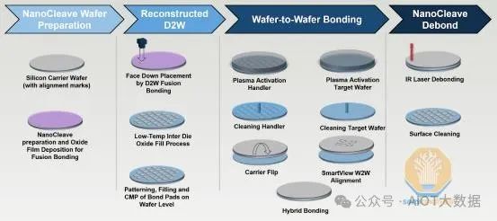
This is actually a simplified process, as the bottom die can also be reconstructed on the carrier wafer. Therefore, both the top and bottom dies are cut from the original silicon wafer and the KGDs are sorted. Both sets of dies are bonded to their respective carrier wafers in precise locations. The two carrier wafers are then bonded together using a W2W process. This is done in TSMC SOIC. Therefore, each AMD 3D V-cache die uses five bonding steps (bottom CPU die to carrier, 3D V-cache die to carrier, and two dummy silicon die to carrier), and wafer-to-wafer bonding.
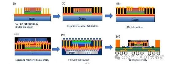
The reconfiguration process can also be used for more extreme heterogeneous integration options.Intel demonstrated "Quasi-Monolithic Chip (QMC)" at IEDM 2022.One example of a QMC application they demonstrated was a package with two heterogeneous integrated chips on the top and bottom. Each chip is attached to a carrier wafer on both the top and bottom sides. The wafer is then molded with a thick inorganic oxide (such as SiO2). W2W bonding is performed. The molded chips are then singulated and attached to the package substrate to complete the process.
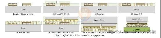
Note that TSVs may exist within the reconstructed area.
Direct D2W bonding involves placing individual dies directly onto the target wafer for pre-bonding. While less mature, direct D2W appears to be poised for increased use in the future due to its simplified process. One benefit of collective D2W is that it can be cleaned and then fed directly into the alignment chamber, reducing contamination. The recent introduction of D2W cluster tools (discussed below) replicates this process, reducing the benefits of this collective process. Furthermore, as alignment becomes more challenging, D2W is more suitable for finer pad pitches, thus eliminating the W2W step, which introduces additional misalignment risk.
Due to the process challenges and cost of D2W hybrid bonding, current adoption is limited. AMD was an early adopter in 2022 and remains the only one to date. We will discuss future applications, adoption rates by company, and the number of process steps later.
One thing to note is that W2W is far ahead of D2W in terms of alignment, so if your design is not heterogeneous and the wafer yield is high enough, it will actually be a more precise and higher-yield process. This finer pitch will also unlock many new use cases that D2W has not yet broken through.
Hybrid bonding process
Let’s take a closer look at the D2W and W2W processes.
TSV formation
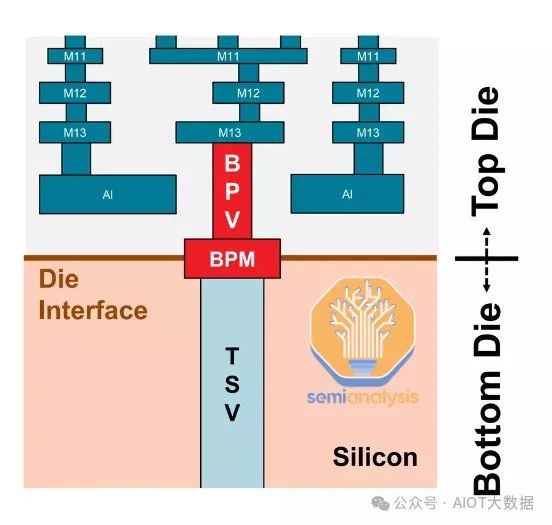
As we mentioned above, TSVs need to provide power and signals to all the chips in the package. Imagine a traditional flip-chip package. The chips only need interconnects on one side to receive power and communicate data with the package substrate. This interconnect layer has bumps that connect to the passive wiring layer (also known as the "metal layer" or "back-end of line"/BEOL). These bumps provide power and signals to the transistor layer that switches and processes data.
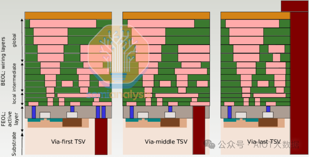
For 3DICs, the bottom die needs to be able to communicate with both the package substrate beneath it and the die above it, so both sides of the die need to be interconnected. This is where TSVs come into play. TSVs come in several varieties, depending on when they are manufactured in the process. TSVs can be "via-first," created in the silicon wafer before the transistor layer; "via-middle," created after the transistor layer is complete but before the metal layer; or "via-last," created after the BEOL (Below-End-of-Line) layer.
The most common for 3DICs is the “through-in-the-middle” approach, as the TSVs run between metal layers, through the transistor layers and out to the backside of the chip, so that now there is a layer of interconnect on both sides of the chip, which we will describe.
We are hereThe TSV process was discussed but will be recapitulated in this report.
The wafer is coated with photoresist and then patterned using photolithography. Deep reactive ion etching (DRIE) is then used to etch the TSVs into the silicon, creating high-aspect ratio trenches deep within the wafer without penetrating the entire wafer. Chemical vapor deposition (CVD) is used to deposit an insulating layer (SiOx, SiNx) and a barrier layer (Ti or Ta). These layers prevent copper from diffusing into the silicon. Physical vapor deposition (PVD) is then used to deposit a copper seed layer. This seed layer is deposited in the trenches, which are then filled using electrochemical deposition (ECD). This forms the TSVs. However, the process is not complete, as the backside vias are not yet exposed. To expose the TSVs, the backside of the TSVs is polished and, in some cases, etched to thin the backside and subsequently expose the TSVs. Once completed, the wafer can proceed to the back-end of the line (BEOL) formation.
The formation of TSVs is not easy and can be very time-consuming, especially due to the deep etching required. We understand that TSV formation is a bottleneck in HBM and CoWoS production. Some customers start with silicon interposers.Moving to CoWoS-ROne reason is to avoid the expensive TSV process in the silicon interposer.
Hybrid bond layer formation
After the wafer bonding interface, a hybrid bonding layer is fabricated on top of the wafer's back-end-of-line (BEOL) layer. This layer is the same for both W2W and D2W fabrication. This layer is a dielectric film patterned with fine-pitch copper vias. The dielectric, typically silicon carbonitride (SiCN), is deposited via PECVD. Bond pads are then formed. Holes for the copper pads are patterned and etched away using photolithography. Barrier and seed layers are deposited, followed by copper plating using a typical copper damascene process.
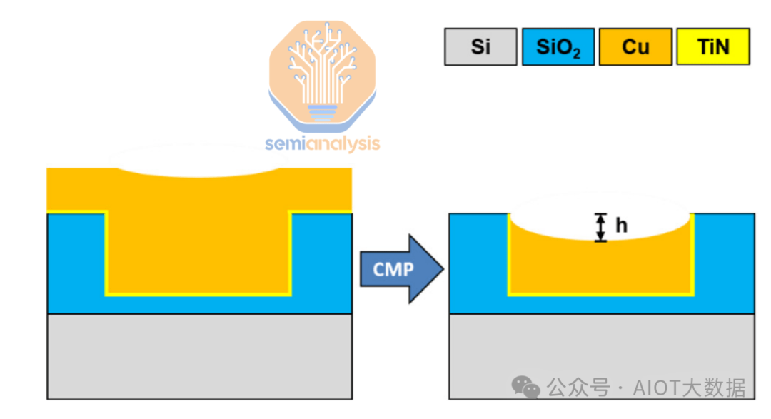
Then, a CMP step is performed to grind and smooth the dielectric surface and obtain the correct copper profile.A notable feature of the copper pads is that they are recessed to approximately 1 micron pitchAs mentioned previously, a smooth surface is essential for forming a good bond.The roughness of the dielectric must be controlled within 0.5nm, and the roughness of the copper pad must be controlled within 1nm。
A characteristic of the HB interface is that the copper pad is initially recessed approximately 5 nm below the dielectric layer. This is to ensure that the copper does not interfere with the initial dielectric-to-dielectric bond during the annealing process.If the copper is recessed too deeply, the Cu-Cu bond may not form properly。
During CMP of copper and other metals, dishing often occurs due to overpolishing and the different softness levels of the metal and dielectric. While not ideal, this phenomenon is not serious and can be addressed. The exact profile of the dishing needs to be controlled to prevent copper overgrowth/undergrowth during bonding.
To achieve the correct recess profile, multiple CMP steps combining low and high Cu removal slurries are required. CMP is a key process for hybrid bonding to achieve very smooth surfaces and optimal profiles.
At ECTC, Sony demonstrated that when the pitch is reduced to 1 micron, having copper protruding is better than having copper recessed.
Wafer sorting/separation
For D2W only, wafer sort is performed, and the KGDs are singulated and reassembled on a carrier wafer or tape frame for further processing. As mentioned above, HB introduces new complexities to the traditional wafer sort process. Wafer sort involves probing the wafer bumps or pads with probes for electrical testing.
Probing can cause small amounts of damage to the copper pad surface, disrupting the smoothness of the surface during the CMP process. While this damage to the pad is minimal and generally acceptable in most cases, HB is very sensitive to small topographic variations, which can affect bond quality. One way to address this is to compensate for this during the initial CMP, then perform another round of post-CMP probing to polish away any damage caused by probing.
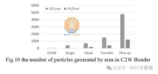
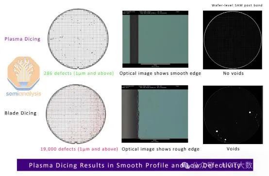
With singulation/dicing, one issue is particles generated during the process.Blade cuttingNot usually used because it is the dirtiest: it produces a lot of particles and causes significant yield loss.Laser cutting and plasma cuttingPreferred over blade dicing because they are cleaner processes, but they still produce particles. Plasma dicing is the most extreme method, with a mechanism similar to etching away the scribe lines that separate the chips. However, this method has a much lower yield given the time required to etch an entire wafer.
Disco is a leader in this space. Their stock has more than tripled since we covered them.
One mitigation technique is to first coat the wafer with a protective layer. Particles land on the protective layer and are removed along with it during stripping. While this helps address particle issues during the singulation process, some protective layer residue may remain, and the stripping process may also cause some surface damage to the HB layer, increasing surface roughness.
Plasma activation and cleaning:
The two wafers are now processed to prepare for bonding. They are treated with N2 plasma to activate the surfaces. The plasma treatment changes the properties of the surfaces, increasing their surface energy and making them more hydrophilic. Making both surfaces more hydrophilic allows them to promote hydrogen bonding.This facilitates initial weak dielectric-to-dielectric pre-bonding, which occurs in the next step at room temperature.
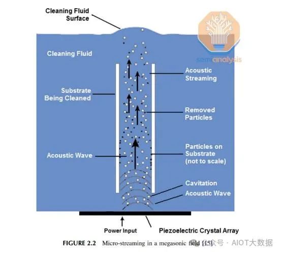
After processing, a final clean is performed to remove any accumulated particles. Prior to bonding, it is important that the incoming wafer is as clean as possible. Cleaning needs to be thorough, but also non-damaging, to maintain the integrity of the HB interface. The best approach appears to be to use a deionized water-based clean supplemented withultrasoundUsing scrubbers or plasma cleaning may cause too much damage and/or introduce contaminants.
Bonding
Now comes the bonding step. More accurately, it's more like "pre-bonding," as this step only forms the initial dielectric-to-dielectric bond, which is a weak van der Waals bond. We'll describe the workflow for both the W2W and D2W methods separately.
W2W bonding
What makes W2W bonding yield higher is the separation of the alignment and bonding steps. First, there are various techniques for W2W alignment. In the past, infrared scanners were used to check alignment between two wafers. However, this limitation was that one wafer had to be transparent to infrared light. This doesn't work for CMOS wafers, as infrared light cannot penetrate metal layers.
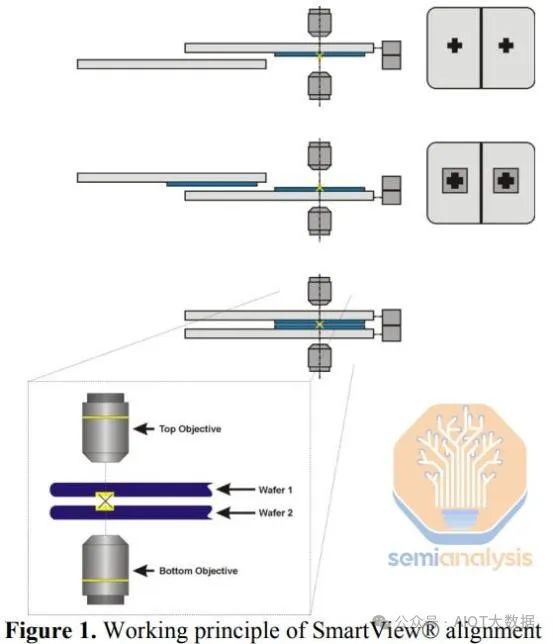
EVG leads the W2W bonding field with its patented SmartView alignment technology. Two cameras are calibrated against each other, one positioned above and one below the target wafer. The chuck holding the top wafer moves so that the bottom camera can identify the alignment marks, and the system records the positions of the alignment marks. The top wafer is retracted, and the bottom wafer is then moved between the cameras until the top camera can identify the alignment marks. The aligner can now align the two wafers by calculating the relative positions of the two alignment marks. To help maintain accuracy and control, the wafers are held very close to each other (within 50 microns), and the chuck moves only in the X and Y planes; the Z axis (vertical) is not moved until pre-bonding.
After alignment, the wafers are moved into a bonding chamber where they are pressed together with light pressure for about 20 minutes to form the initial bond.
Post-bonding inspection can be done on site by acoustic methods and re-bonding can be performed if alignment is inadequate.
In a W2W tool, a separate chamber is used to perform alignment. Once the top and bottom wafers are aligned, they are moved into the bonding chamber (under vacuum), where they are pressed together with minimal force. After approximately 20 minutes, the initial pre-bond is formed. The key to W2W is that it is a cleaner process because there are fewer steps. Before alignment and bonding, the wafers can be cleaned to remove most particles. Die separation, a source of particle contamination, occurs only after bonding.
Since this is a wafer-level process, the alignment step also has more time, so the longer alignment time does not affect the yield as much as the chip-level process. There is also not much movement in the chamber, so there is less contamination generated in the chamber. Currently, W2W bonders can achieveAlignment accuracy below 50nmW2W bonding is a mature process with low cost. As evidenced by its widespread adoption in mass-market products, such as image sensors from Sony, Omnivison, and Samsung, and NAND from Yangtze Memory Technologies, Western Digital, and Kioxia.
D2W bonding
D2W bonding is accomplished with a pick and place tool.
The bottom target wafer rests on the wafer chuck. The die to be bonded is placed face-up on the tape frame. A flip arm collects the individual die and flips it over, placing it back-side-up on the flipper. A bonding arm above picks up the flipped die using vacuum suction on the bonding head.
Key manufacturing steps for CoWoS-S (primary variant)
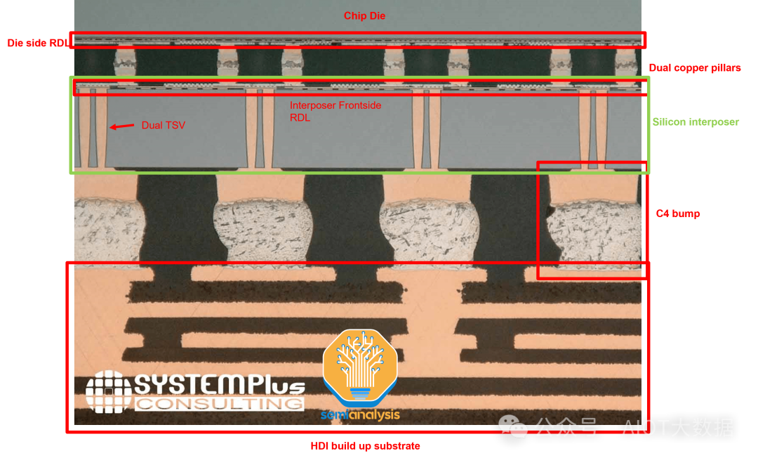
CoWoS is a TSMC "2.5D" packaging technology in which multiple active silicon dies (typically configured as a stack of logic and HBM) are integrated on a passive silicon interposer. The interposer acts as a communication layer for the active die on top. The interposer and active silicon die are then connected to a substrate containing I/O for placement on a system PCB.It is the most popular packaging technology for GPUs and AI accelerators because it is the primary method for co-packaging HBM and logic to achieve optimal performance for training and inference workloads.
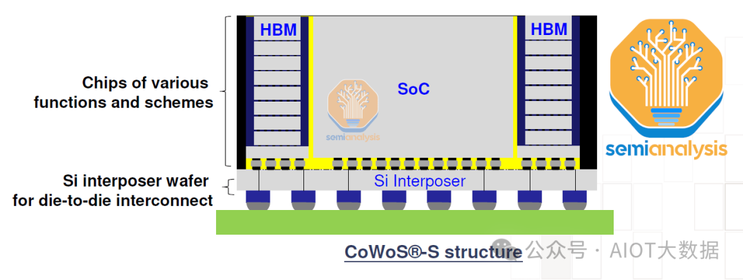
We will now detail the key fabrication steps of CoWoS-S (primary variant).
Key process steps of silicon interposer
The first step is fabricating the silicon interposer, which contains the "wiring" that connects the chips. Fabrication of this silicon interposer is similar to traditional front-end wafer fabrication. It's often claimed that the silicon interposer is manufactured using 65nm process technology, but this is inaccurate. The CoWoS interposer contains no transistors, only metal layers, suggesting a similar metal pitch, but this is not true.
This is why 2.5D packaging is often done in-house by leading foundries, as they can produce the silicon interposer while also having direct access to cutting-edge silicon. While other OSATs like ASE and Amkor have done advanced packaging similar to alternatives like CoWoS or FOEB, they must source the silicon interposer/bridge from foundries like UMC.
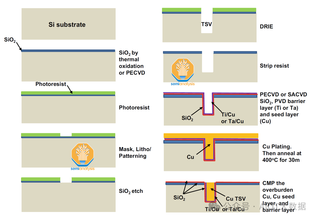
Silicon interposer fabrication begins by taking a blank silicon wafer and creating through-silicon vias (TSVs). These TSVs penetrate the wafer to provide vertical electrical connections between the active silicon (logic and HBM) on top of the interposer and the PCB substrate on the bottom of the package. These TSVs are how the chip sends I/O to the outside world and how it receives power.
To form TSVs, photoresist is applied to the wafer and then patterned using photolithography. Deep reactive ion etching (DRIE) is then used to etch the TSVs into the silicon, achieving a high aspect ratio. Chemical vapor deposition (CVD) is used to deposit an insulating layer (SiOx, SiNx) and a barrier layer (Ti or TA). Physical vapor deposition (PVD) is then used to deposit a copper seed layer. Electrochemical deposition (ECD) is then used to fill the trenches with copper to form the TSVs. The vias do not pass through the entire wafer.
After TSV fabrication, a redistribution layer (RDL) is formed on top of the wafer. Think of an RDL as a multilayer wiring layer that connects the various active chips together. Each RDL consists of a smaller via and the actual RDL.
Silicon dioxide (SiO2) is deposited via PECVD, followed by a photoresist coating. The RDL is patterned using photolithography, and then the silicon dioxide is removed from the RDL vias using reactive ion etching. This process is repeated multiple times to form a larger RDL layer on top.